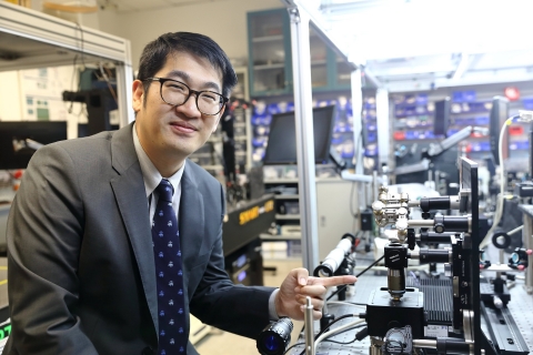
Ultraprecise 3D printing technology is a key enabler for manufacturing precision biomedical and photonic devices. However, the existing printing technology is limited by its low efficiency and high cost. Professor Shih-Chi Chen and his team from the Department of Mechanical and Automation Engineering collaborated with the Lawrence Livermore National Laboratory to develop the “Femtosecond Projection Two-photon Lithography (FP-TPL)” printing technology. By controlling the laser spectrum via temporal focusing, the laser 3D printing process is performed in a parallel layer-by-layer fashion instead of point-by-point writing. This new technique substantially increases the printing speed by 1,000 - 10,000 times, and reduces the cost by 98%. The achievement has recently been published in Science, affirming its technological breakthrough that leads nanoscale 3D printing into a new era.
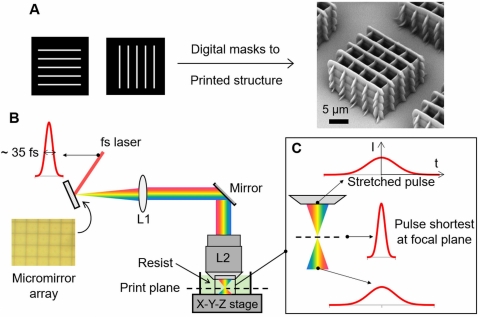
The conventional nanoscale 3D printing technology, i.e., two-photon polymerisation (TPP), operates in a point-by-point scanning fashion. As such, even a centimeter-sized object can take several days to weeks to fabricate (build rate ~ 0.1 mm3/hour). The process is time-consuming and expensive, which prevents practical and industrial applications. To increase speed, the resolution of the finished product is often sacrificed. Professor Chen and his team have overcome the challenging problem by exploiting the concept of temporal focusing, where a programmable femtosecond light sheet is formed at the focal plane for parallel nano-writing; this is equivalent to simultaneously projecting millions of laser foci at the focal plane, replacing the traditional method of focusing and scanning laser at one point only. In other words, the FP-TPL technology can fabricate a whole plane within the time that the point-scanning system fabricates a point.
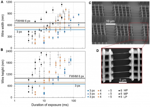
What makes FP-TPL a disruptive technology is that it not only greatly improves the speed (approximately 10 – 100 mm3/hour), but also improves the resolution (~140 nm / 175 nm in the lateral and axial directions) and reduces the cost (US$1.5/mm3). Professor Chen pointed out that typical hardware in a TPP system includes a femtosecond laser source and light scanning devices, e.g., digital micromirror device (DMD). Since the main cost of the TPP system is the laser source with a typical lifetime of ~20,000 hours, reducing the fabrication time from days to minutes can greatly extend the laser lifetime and indirectly reduce the average printing cost from US$88/mm3 to US$1.5/mm3 – a 98% reduction.
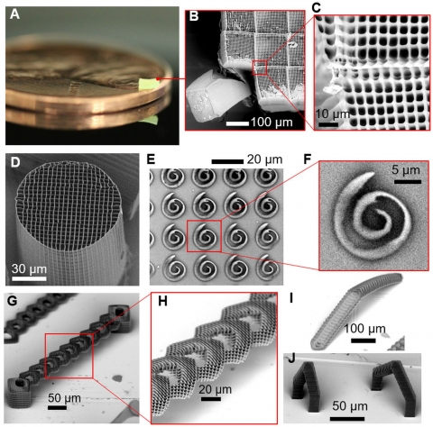
Due to the slow point-scanning process and lack of capability to print support structures, conventional TPP systems cannot fabricate large complex and overhanging structures. The FP-TPL technology has overcome this limitation by its high-printing speed, i.e., partially polymerised parts are rapidly joined before they can drift away in the liquid resin, which allows the fabrication of large-scale complex and overhanging structures, as shown in Figure 1 (G). Professor Chen said that the FP-TPL technology can benefit many fields; for example, nanotechnology, advanced functional materials, micro-robotics, and medical and drug delivery devices. Because of its significantly increased speed and reduced costs, the FP-TPL technology has the potential to be commercialised and widely adopted in various fields in the future, fabricating meso- to large-scale devices.
The research team has been supported by the Innovation and Technology Commission (ITC), receiving multiple Innovation and Technology Fund (ITF). The project also received support from the Lawrence Livermore National Laboratory, under the Department of Energy of the United States. The research team has received multiple U.S. patents related to this project and the results were published in Science in October. Science is regarded as one of the most prestigious academic journals in the world, published by the American Association for the Advancement of Science (AAAS).


